
What is a silicon wafer?
A silicon wafer is a circular thin plate (wafer) processed from a single crystal ingot made of polysilicon (high purity polycrystalline silicon).
By further processing this silicon wafer, various semiconductor devices are manufactured from individual semiconductor elements such as diodes and transistors to integrated circuits (ICs).
Silicon wafers are indispensable parts for the manufacture of semiconductor substrates and solar cells mounted on electronic products such as personal computers, smart phones, and other home appliances.
Without them, modern life as we know it would be very different.
The process of making silicon wafers
Here is the process of making silicon wafers from polysilicon.
In addition to what we introduced here, we have various processing methods.
We can respond to customer's request if the wafers need to be manufactured from the ingot.
 Pull up
Single crystal ingots are manufactured from polysilicon (polycrystalline silicon) which are raw materials for silicon wafers.
First of all, polysilicon and raw materials for adjusting the electrical resistivity of the semiconductor are melted in a quartz crucible.
Next, when seed crystal silicon rod is put in liquid state silicon and pulled up, ingots are grown.
![]()
 Various machining
Slicing (cutting)
The pulled single crystal ingots are grinded so that the diameter becomes uniform.
They are sliced a thickness of about 1 mm by using a blade or a wire saw to process it into a wafer shape.
Beveling
By chamfering the sliced wafers, chips and cracks can be prevented.
Lapping
While securing thickness variation, we roughly lap the surface with alumina abrasive which eliminates distortion and makes the thickness smooth.
![]()
 Etching
Any distortion and damage caused by lapping so far, impurities remained on the wafer surface, etc. are removed by chemical etching.
![]()
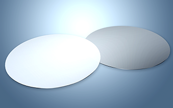
 Polishing
The surface of the wafer is polished improve the flatness and is given a mirror finish.
It is polished by fine abrasive grains and polishing pads with thicknesses of about several millimeters.
![]()
 Cleaning / Inspection
Production is completed after being washed and then being put through a rigorous inspection.
The ultra-high quality silicon wafers produced are used in various electronic components all over the world.
